We're happy to introduce the Fraunhofer IZM, a research institute that is a part of the Fraunhofer-Gesellschaft, that specializes in applied and industrial research in packaging technologies and integrating multifunctional electronics into systems. With over 400 employees across four departments, it provides expertise in microelectronics packaging from concept to reliability.
The Fraunhofer IZM's microLED project is led by Dr. Oppermann, IZM’s Deputy Head of Department and Dr. Manier, R&D project engineer. Dr. Opperman has led the "Fine Pitch Assembly and Interconnects" group at Fraunhofer IZM since 1999, focusing on flip chip, die attach, and wafer-level packaging for MEMS, RF, opto, and power applications. His innovations include AuSn soldering, transient liquid phase bonding, nanometal bonding, and Indium bonding. Dr. Manier has contributed to flip chip and die bonding technologies in MEMS, power electronics, and medical applications. He has been involved in European and industry projects, including chip-to-chip/substrate bonding and vacuum-tight MEMS sealing.
Dr. Oppermann and Dr. Manier recently finalized a techblick feasibility study into microLED massive parallel assembly and interconnection.
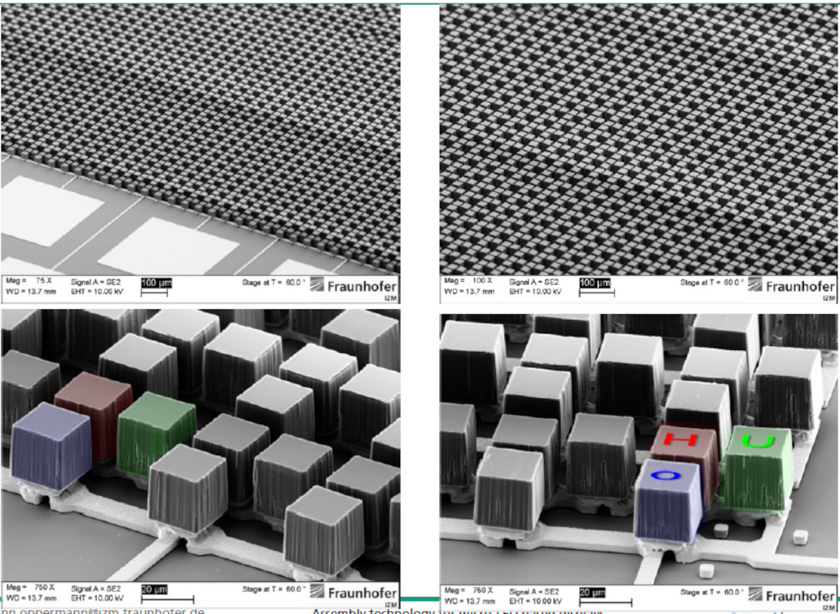
Fig 1. SEM imaging of assembled micro-display of Figure 1 with 3 different small die (RGB) soldered on target substrate
Hello Dr. Oppermann and Dr. Manier, can you introduce Fraunhofer IZM 's microLED technology?
Fraunhofer Institute for Reliability and Microintegration (IZM) is a research institution based in Berlin, Germany renowned for its research work in microelectronic packaging and wafer level packaging with more than 30 years of expertise. With one of the first public R&D cleanroom for WLP in Germany and as pioneer in these domains, Fraunhofer IZM focuses on developing advanced solutions that drive innovation and enhance the performance and reliability of microelectronic systems. The institute topics cover a broad range and aspects of microelectronic packaging technologies – from wafer processing to reliability testing and environmental aspects- with two main process platforms: square substrates PCB and Panels as well as round – wafer.
Can you say why you joined the MicroLED Industry Association and what it is you hope to achieve?
One of our mission is to develop technologies and processes to be at the cutting edge of the technological innovation, providing solutions that meet the ever-evolving needs of the electronics industry. MicroLED Displays represent an exciting topic since the entire assembly path remains highly challenging, especially the aspects around assembly and electrical interconnects. As such, it is of value for Fraunhofer IZM to participate to the MIA, to be at the nearest of the technological evolution, stay informed on related topics and possibly identify collaborations, where we might propose our technological support.
What are your biggest challenge and success to date in the microLED industry?
We developed with µLED-Mockups (mechanical Silicon microchips) a process specific to the assembly of MicroLEDs onto substrates mimicking micro display. This involves 1/ selective picking and massive parallel transfer enabling safe and precise manipulation of (sub)array of such tiny dies and 2/ the assembly itself onto the target substrate, i.e. backplane microdisplay, inclusive electrical connections using micro-bumps. As a first technological tentative, we demonstrated finally its feasibility by succeeding in 99% yield at lab scale of more than 16.000 LEDs reconfigurated in three sub-arrays and electrically connected, with chip size of 23 µm separated by a gap of 8µm.
Can you detail your latest prototype/demonstration?
Basically, this demonstration relies on LED back end preparation, especially the face up IOs with AuSn Bumping, combined to the flip of the entire device wafer using a first temporary carrier and adhesive. This step permits the detachment of the epitaxy substrate at wafer level. Afterwards, a second temporary carrier, we called conveyor, is attached to the revealed LED backside, to selectively pick the MicroLED die in array from the donator. This process is laser-assisted to detach the microLEDs from the donator. After transfer to the conveyor, the picked microled array is aligned to the target substrate, i.e. the backplane, and electrically bonded using gold-tin solder. Then the conveyor is detached using the laser process. The sequence is repeated for green and blue LED source wafer, enabling RGB onto the display. Within the entire procedure, the MicroLEDs are constantly firmly maintained to keep the array intact and plane and avoid any die shift. The AuSn bonding present the biggest advantage to be insensitive to further thermal budget in the downstream process flow / next level integration. This work is going to be published in the ESTC 2024 conference.
Fig 2. 4.6x4.6 mm² display substrate with 150x150 array of 3 different types of 20 µm chips soldered onto.
Paper: C-A Manier, K. Zoschke, H. Oppermann; Massive Parallel Assembly and Interconnection for Micro-LEDs – a Technical Feasibility Study; ESTC 2024, Berlin, to be published online at IEEE
How do you see microLEDs changing the display industry in the next 5-10 years?
MicroLEDs are moving from lab to industry since back to 10 years. Shortly, we think Microled Displays make sense with microchips, under 10µm edge size, especially for small displays. In this direction, handling and transfer technologies make large progress in the last 5 years. There are still pros and cons in the use of lateral (P and n on same device side) or vertical (P up, N down) MicroLEDs in terms of assembly, with also different technical approaches for backplane population. To our knowledge, a technological breakthrough is not solely depending onto the adoption by the LED maker industry of one or the other LED topology, but depend onto the complete assembly scheme. Upscalings for throughput and yield are determinant in terms of production. The one who will succeed in bringing the proper electrical interconnect technology for millions of LEDs - in ultra dense arrays as well as relaxed arrays for large screens - to the backplane will not only highly impact the MicroLED ecosystem but potentially also the chiplet integration.