Submicron LEDs

Polar Light Technologies demonstrated a red pyramidical GaN microLED array, thus achieving RGB microLEDs on the same material platform

Pyramidical GaN microLED developer Polar Light Technologies announced that it has managed to produce red (625 nm) microLEDs based on its non-etching bottom-up platform. The company now has demonstrated the production of red, green and blue pyramidal microLEDs using the same material compound. 

Red is the most challenging microLED emitter, and companies have been looking at several alternatives to native GaN red microLEDs, including 3D nanowires, color conversion, and color tunable LEDs.  Polar Light Technologies’ microLED is composed of pyramid shapes that are built with a novel bottom-up approach, a technology that the company says comes with unique benefits, including reduced strain in the lattice of the InGaN/GaN structure, a unique possibility of frontplane integration, no etching damage (and so higher efficiency), ability to produce small microLEDs, even sub-micron, a narrow emission cone and more. 

Read the full story Posted: Dec 21,2024

Researchers from Kookmin University developed new GaN submicron Fin-LEDs, and a face-selective dielectrophoretic assembly process

Researchers from Korea's Kookmin University have developed a new GaN-based fin-LED chip material and pixel process technology, saying that this innovation may be the key to overcome the limitations of current microLED technologies.

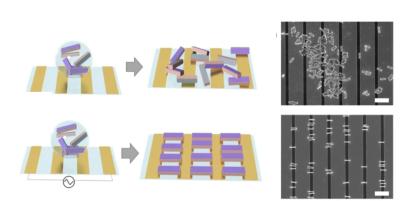
The researchers developed a viable pixel manufacturing process that vertically assembles sub-micron-sized fin-LEDs using a face-selective dielectrophoresis (DEP) assembly method. The GaN-based sub-micron-sized fin-LEDs are designed to maximize performance while minimizing costs related to the chips and pixelation process. This technology significantly enhances extraction light efficiency by vertically aligning the fin-LEDs, and it enables the implementation of chip materials and pixel manufacturing processes that significantly reduce production costs.

Read the full story Posted: Nov 06,2024

The MicroLED Industry Association to host a sub-micron LED webinar

On February 17th 2025, the MicroLED Industry Association will host a private webinar focused on submicron LED technology. During this webinar, association members will look into sub-micron LED technology, understand the latest status and research innovation and discuss how submicron LEDs should take part in the future microLED industry.

The webinar will feature two speakers, and will follow with an open Q&A session.

Read the full story Posted: Oct 30,2024

Researchers develop a top-down method to produce high-efficiency sub-micron microLEDs.

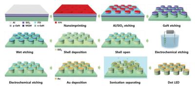
Researchers from Korea's Kookmin University in Seoul, led by Prof. Young Rag Do, have developed a novel top-down process to fabricate and isolate sub-micron GaN microLEDs. The process combines electrochemical etching and sonochemical separation of the etched porous layer to isolate the microLEDs.

The researchers have used the process to produce Au-coated GaN blue LEDs that offer an EQE of 6.21% (at 4.0 V) and a luminous efficacy of 1,070 cd/m2 (at 10.0 V). The LEDs themselves had a diameter of 750 nm, these are true sub-micon LEDs.

Read the full story Posted: Oct 24,2024

Polar Light Technologies and Finetech collaborate on microLED production technologies

Pyramidical GaN microLED developer Polar Light Technologies announce a partnership with die bonding solution developer Finetech, to co-develop microLED technologies. The two companies already started developing microLED microdisplay applications. 

Polar Light Technologies and Finetech developed a modified flip-chip cold bonding technique that ensures accurate alignment between the microLEDs and the electronics. The two companies say that in early trials, this method showed an impressive 85% success rate, proving its potential for large-scale manufacturing.

Read the full story Posted: Sep 19,2024

Hummink's biz-dev VP shares his views on the microLED industry and details his upcoming talk at MicroLED-Connect

France-based Hummink develops high percussion capillary printing technology, that enables a highly controlled and prices (sub-micron scale) deposition of materials. The company's VP Business Development, Dr. Frederic Raynal, will give a lecture at the upcoming MicroLED-Connect virtual webinar on November 2023, and was kind enough to answer a few questions we had.

Hello Dr. Raynal. Can you give us a short intro to your company and microLED product/service?

Hummink is the leading developer and supplier of High Precision Capillary Printing (HPCAP), a revolutionary technology in many applications including the display and semiconductor industry. Spun-off from world-renowned research institutes, the company is based in Paris, with representatives in key regions (Korea, US, Taiwan, Japan, Europe). HPCAP involves the controlled deposition of materials, achieving high pixel densities with accurate alignment at extremely small sizes (sub-micronic scale), which is mandatory for the manufacturing of current and future generations of MicroLED. Hummink is a technology provider, enabling customers to have access to both equipments and inks through a single partnership.

Read the full story Posted: Oct 27,2023

Mojo Vision closes its Series A funding round, raising $43.5 million to accelerate its microLED microdisplay technology development and commercialization

MicroLED developer Mojo Vision announced that it has closed its Series A funding round, raising $43.5 million. In April 2023 the company announced the first trench of its Series A funding ($22.4 million), which means that the company now raised $21.1 million.

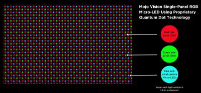
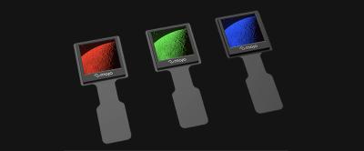
Mojo Vision R/G/B microled microdisplays

This round was led by long-time investors (New Enterprise Associates and Khosla Ventures) and new investors (Vanedge Capital) with participation from several investors including Shanda Grab Ventures, Dolby Family Ventures, Advantech capital and Fusion Fund.

Read the full story Posted: Oct 12,2023

A spotlight on GE: a MicroLED Industry Association member

We're happy to interview GE, as part of our series of interviews with MicroLED Industry Association members. GE offers narrow band red and green phosphor technologies known as KSF and PFS, suitable for microLED color conversion.

Can you introduce your company and technology?

Rachel Cassidy, PhD, MBA: The General Electric Company (GE) is an American multinational company. For more than 125 years, GE has invented the future of industry. Today, GE is best known for its work in the Power, Renewable Energy, Aviation and Healthcare industries.

GE’s Licensing team provides access to GE’s patent portfolio and technical and intellectual resources. Licensees receive world-leading technology paired with advice and guidance to accelerate their technology development and achieve market differentiation.

The GE LED Phosphors team has world class chemistry and physics expertise as well characterization capabilities that have resulted in commercial successes in both lighting and LCD display technologies. Multimillion-dollar yearly revenue, multiple awards, hundreds of patents, over 20 licensees of our patents, along with various publications and invited conference presentations show that this team is on the cutting edge of luminescent material development and can advance from concept to invention to commercialization. Our narrow band red phosphor technology known as KSF (K2SiF6:Mn) can be found in over 60 billion LEDs as well as remote films for miniLED applications sold into the display industry.  The great success of KSF phosphor in the display industry is due to the high color gamut and energy efficiency that has best in class reliability.

Read the full story Posted: Sep 18,2023

Mojo Vision developed the world's highest density red microLED microdisplay

AR microLED microdisplay developer Mojo Vision announced that it has developed the world's highest-density (1.87 um pixel pitch) red (620 nm) microLED microdisplay. Mojo produced a first working prototype of its display, that is based on 1.37 um blue LEDs with QD color conversion

Last month Mojo announced that it has achieved a process milestone and has lit-up its first 300 mm GaN-on-Silicon blue microLED array wafer. The company said it is on track to maturing its 300 mm CMOS fab process.

Read the full story Posted: Jun 28,2023