November 2023

Tianma developed a 1.63" microLED wearable display

During the company's latest innovation conference, Tianma unveiled that it developed a small 1.63" 403 PPI microLED display, that targets wearables and small mobile terminals.

The company did not disclose more information on this new display, and did not say how close it is to commercialize it.

Read the full story Posted: Nov 30,2023

Q-Pixel developed the world's smallest full color microLED pixel, and demonstrated a 10,000 PPI display

US-based Q-Pixel announced that it has developed the world's smallest full-color pixel (1 micron) and demonstrated a 10,000 PPI microLED microdisplay based on its proprietary tunable polychromatic microLED technology (which it brands as TP-LED). 

Q-Pixel's technology enables a single-pixel color-tunable microLED device, and the company's displays are produced using a monolithic process. In May 2023, the company announced a 5,000 PPI full-color microdisplay, so this is fast progress only a few months later. Q-Pixel is a MicroLED Industry Association member.

Read the full story Posted: Nov 30,2023

Exaddon launches 20um 3D printed probes for microLED testing

Exaddon developed a unique micro 3D Printing technology that enables it to produce probes that can access and test pads and bumps with pitches of less than 20 micron. The company says that this unique method halves the current limit of fine-pitch probing, enabling microLED developers testing options that haven't been available before.

Exaddon's μ3D printing technology delivers high quality printed metal with micrometer resolution. Exaddon’s initial microLED test array is 3D printed directly on prepatterned traces with a pitch of less than 20 μm; This demonstrator validates Exaddon’s process on microPCBs for mounting on current probe heads. With 128 probes, the array gives microLED testers a 64x increase in efficiency.

Read the full story Posted: Nov 22,2023

The MicroLED Industry Association to host an in-person dinner during MicroLED Connect 2024 in Eindhoven

The MicroLED Industry Association announces a members-only dinner meeting at MicroLED Connect 2024, in Eindhoven, The Netherlands, on September 24, 2024.

This will be a casual dinner that will give members a great opportunity to relax, have fun and network in a friendly and free environment. This dinner will be the 2024's second in-person meeting for the MicroLED Industry Association, with the first one planned for SID Displayweek 2024.

Read the full story Posted: Nov 22,2023

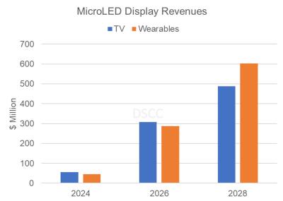
DSCC: the microLED display market to reach $1.4 billion by 2028, led by TV, wearables, automotive and AR displays

DSCC estimates that the microLED display market will reach $1.4 billion by 2028, led by TVs and wearables. Other applications will include AR glasses and automotive displays (these do not appear in the graph below).

DSCC believes that MicroLED displays will offer superior performance, but its high price will keep it from being a mainstream technology in the near future. The first microLED smartwatch will launch in 2024, but it will target the high-end of the market and volumes will remain low. 

Read the full story Posted: Nov 21,2023

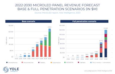
Yole sees significant microLED production in 2-3 years, with broader adoption in 5-10 years

Yole Intelligence has published its latest microLED market report, in which it sees commercial microLED production starting in 2-3 years, following several delays. In 5-10 years, adoption will increase.

In its base scenario, Yole sees microLED panel sales reaching $1.5 billion in 2029 and $2.2 billion in 2030, with almost 90% coming from wearables and AR/VR/MR microdisplays. The rest of the panels will be used in TV applications. If you want to hear more about Yole's microLED market insights, you are welcome to join the MicroLED-Connect online event later this month.

Read the full story Posted: Nov 16,2023

A spotlight on the Fraunhofer FEP: a MicroLED Industry Association member

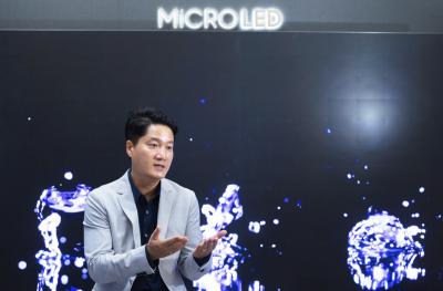
We're happy to interview Dr. Uwe Vogel, the Deputy Director of the Fraunhofer FEP and the Division Director of the Fraunhofer's Microdisplays and Sensors division, as part of our series of interviews with MicroLED Industry Association members. The Fraunhofer Institute for Organic Electronics, Electron Beam and Plasma Technology (Fraunhofer FEP) is located in Dresden, Germany, and focuses on developing innovative solutions, technologies and processes for surface modification and organic electronics.

Hello Dr. Vogel. Can you introduce your company and technology?

The Fraunhofer Institute for Organic Electronics, Electron Beam and Plasma Technology FEP is one out of 76 institutes and research units of the Fraunhofer-Gesellschaft e. V., the largest European institution for applied research. The core competences of Fraunhofer FEP are electron beam technologies, vacuum thin film deposition techniques and technologies for organic electronics, microdisplay technology and sensors. Main activities target development and adaption of the thin film deposition technologies to a wide range of industrial applications. Fraunhofer FEP runs multiple pilot-scale vacuum coating systems.

Read the full story Posted: Nov 15,2023

MicroLED presentations from last year's microLED virtual meeting from UCSB, Coherent and Yole Intelligence

MicroLED-Connect is an upcoming hybrid event series, a year-long program of virtual and onsite events, all focused on the microLED industry. The first MicroLED Connect virtual event is coming up later this month, a 2-day virtual event that will be focused on microLED (and also miniLED) technologies. The event will include over 25 lectures from leading companies, researchers and market analysts. The series is organized by the MicroLED Industry Association together with TechBlick.

In this post we share three online presentations, taken from last year's online microLED event (November 2022). The first video, above, is from the SSLEEC group (led by Prof. Denbaars and Prof. Nakamura) at the University of California, Santa Barbara, that discusses the latest microLED research performed at this world-renowned group. 

Read the full story Posted: Nov 15,2023

How seamless are microLED tiled TV displays?

Samsung, Sony, LG and others are producing commercial microLED panels, mostly for ultra-premium, signage and commercial applications. The ultra-large size displays are made from small microLED modules, seamlessly tiled together.

MicroLED technology makes it possible to connect two tiles in a way that retains exactly the same pixel pitch even at the tile connection (this is something that is challenging to do with OLED or LCD displays). When the displays are active, it is indeed very difficult to spot the seam. When the display is completely black however, this is not the case, and the seams are visible, and the different modules (which are never 100% aligned) reflect light a bit differently which creates a mosaic-like image.
Read the full story Posted: Nov 13,2023