By: Dr. Tali Hurvitz, VP Research & Development & Noam Shapiro, VP Communications, InZiv
MicroLED technology is transforming the world of displays, from AR/VR devices to cutting-edge automotive applications. However, in order for microLED to mature both technologically and commercially, precise functional inspection continues to be essential. Photoluminescence (PL) and electroluminescence (EL) are two primary techniques for evaluating microLED functionality. PL testing measures light emitted from the microLED after excitation by a laser. This excitation mechanism causes a recombination across the entire junction (usually multiple quantum wells, depending on the excitation wavelength) which in turn leads to the emission of light. In this way, PL can measure certain basic properties of functionality.
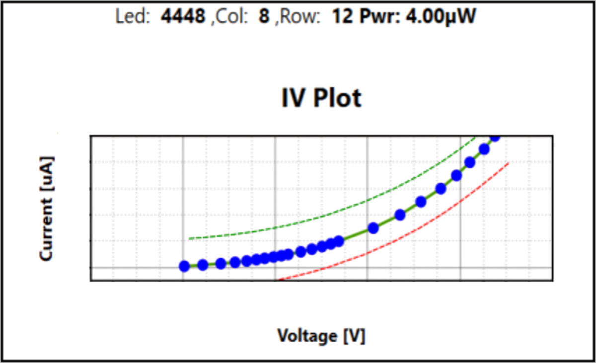
IV (current-voltage) curve being measured during EL testing of a microLED chip
On the other hand, EL testing measures light emitted when voltage is applied to the LED, and in this case, the mechanism that activates the emission of light is the electrons and holes moving to the junction. Because electrons move much faster than holes, most electron-hole recombination—and thus light emission—occurs in the region of the junction where the holes are concentrated. This method of light excitation more accurately reflects real-world performance under operational conditions; the microLED display in the final electronic device will be activated via electric current and not via light.
Research has shown that EL is ultimately the superior method, and relying on PL alone, even while calibrating for inaccuracies, is an unreliable approach that often completely misidentifies defective LEDs as functional, and severely compromises measurement accuracy. Moreover, PL also often mischaracterizes the optical power and wavelength distribution across the wafer, failing to provide reliable testing results. We will briefly summarize below some of the research that has demonstrated the superiority of EL over PL for microLED testing and inspection.
InZiv Research
Internal InZiv research has demonstrated that EL testing is much more accurate and reliable than PL, as PL tends to produce a high rate of “false positives”. In other words, it often misses significant swaths of defective regions, misleadingly identifying these regions as operational, even though under real-world electrical excitation, the LED, or part of it, would not be activated. Therefore, using PL alone risks missing a significant percentage of the defective areas of the microLED, incorrectly classifying them as functional.
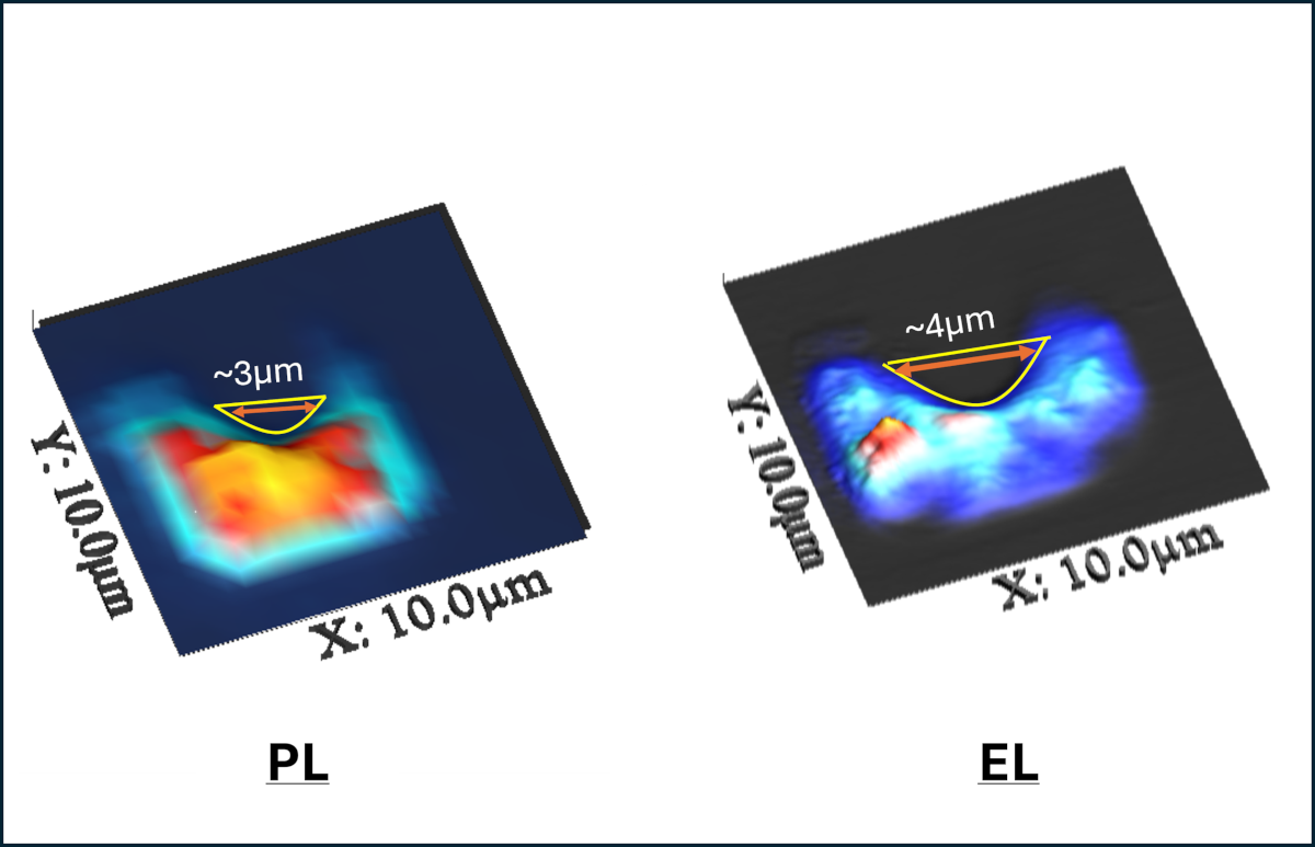
In the optical-topographical image seen above, a microLED chip is excited with PL and with EL. The region of defect is much larger in the EL imaging of the light emission, due to the electro-optical process described above. Under PL testing, those defective areas are excited because of the higher number of electrons that are activated by the laser light, and thus the true defective nature of those regions remains undetected. Only in the EL image, where light is emitted as a direct result of voltage, is the full extent of the defective region exposed. Moreover, as indicated by the larger blue regions in the EL image, the intensity is much weaker when tested with EL. InZiv's findings highlight that while PL can be useful for preliminary diagnostics, it fails to capture critical defects that only EL testing reveals – in this case up to ~30%.
Academic Results
Research from Dr. Kyuheon Kim, Jung-Hoon Song, et al (Kongju National University) provides further evidence supporting the superiority of EL. In the study, two microLED chips were produced using the same process (recipe) —Chip A and Chip B. Yet, they exhibited dramatic differences under PL and EL analysis. The research team proposed identifying a correlation correction function in order to calibrate for this difference. The hypothesis was that once a steady correlation function could be determined between PL and EL, PL could be used and then the results could be calibrated to recreate what the more accurate EL results would have been. However, this too proved elusive. The two chips were tested with EL, and the peak wavelength was identical. This was not the case with PL. Despite their identical fabrication, the two chips exhibited different peak wavelength measurements when they were excited via PL, with a variance of several nm. In other words, the variance between PL and EL was itself inconsistent and varied from chip to chip. Accordingly, no correlation function could be established. A similar inconsistency was found with regard to the optical intensity. Additionally, the research highlights the issue of electron leakage, where electrons escape the quantum wells without recombining, thereby reducing efficiency. This defect remains invisible to PL but is clearly detected through EL testing. The conclusion is thus that EL is in fact indispensable for accurately determining LED health and functionality.
In a separate study, Dr. Keith Behrman, Dr. Ioannis Kymissis, et al, (Columbia University) compared PL, CL (cathodoluminescence), and EL testing on 25 microLEDs. While PL found no defects, EL revealed that 5 of the microLED chips (i.e. 20%) were in fact faulty. This stark difference once again demonstrates that relying solely on PL could result in a 20% defect escape rate.
High Throughput Non-Damaging EL Inspection
InZiv has been a pioneer in microLED testing and Inspection since 2019. The InZiv R-EL Glide is a high-throughput EL inspection system for microLED wafers, featuring unprecedented high speed EL measurements of up to 6,000,000 LEDs per hour. Patented contact probe technology makes contact with the wafer for true EL excitation, but without causing any damage to the wafer. Thousands of repeated scans have proven this unique non-damaging contact capability. The system provides critical data for every individual LED, both optical and electrical, including go/no-go functionality, intensity, wavelength, current voltage, forward voltage, and reverse current curves, all measured with user defined thresholds. Proprietary AI algorithms analyse this data to identify defects and provide actionable insights. Comprehensive reports are generated and seamlessly integrated with fab databases, empowering data driven decisions and optimizing the microLED production process.
Leaders across the microLED supply chain, including microLED research developers, microLED wafer manufacturers and microLED display manufacturers, are discovering the indispensability of EL measurements as part of their inspection process and yield improvement efforts. While PL offers some value for preliminary diagnostics, it falls short when assessing real-world performance. EL testing, on the other hand, uncovers otherwise hidden defects, provides critical insights into efficiency and reliability, and catches early-stage, on-wafer defects – before the microLEDs are transferred to the backplane – thereby empowering microLED manufacturers to further advance in microLED design, to improve yield and to cut costs. As the AR and automotive sectors drive higher performance requirements, automated high-speed EL testing is quickly becoming an industry benchmark and an essential element for achieving the highest standards in microLED testing and inspection.