Native red

Polar Light Technologies demonstrated a red pyramidical GaN microLED array, thus achieving RGB microLEDs on the same material platform

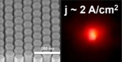
Pyramidical GaN microLED developer Polar Light Technologies announced that it has managed to produce red (625 nm) microLEDs based on its non-etching bottom-up platform. The company now has demonstrated the production of red, green and blue pyramidal microLEDs using the same material compound. 

Red is the most challenging microLED emitter, and companies have been looking at several alternatives to native GaN red microLEDs, including 3D nanowires, color conversion, and color tunable LEDs.  Polar Light Technologies’ microLED is composed of pyramid shapes that are built with a novel bottom-up approach, a technology that the company says comes with unique benefits, including reduced strain in the lattice of the InGaN/GaN structure, a unique possibility of frontplane integration, no etching damage (and so higher efficiency), ability to produce small microLEDs, even sub-micron, a narrow emission cone and more. 

Read the full story Posted: Dec 21,2024

Kubos Semicondcutors raised $2 million to accelerate the development of its cubic GaN technology

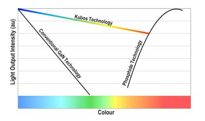
UK-based Kubos Semiconductors announced that it has raised $2 million, to accelerate the development of its cubic GaN technology. This brings Kubos' total funding to $5.5 million, and will enable Kubos to enter the microLED display market within three years through IP licensing. 

Kubos Semiconductors bridging the green gap

In 2023, Kubos announced that it has been granted its first process technology patents and has received its first customer order. It also received an Innovate UK Future Economy Investor Partnerships grant , a 24-month project to achieve 5% efficiency for red microLEDs by deploying the company’s proprietary cubic Gallium Nitride (GaN) process, called KubosLED.

Read the full story Posted: May 07,2024

Ingantec announces an exclusive patent license agreement with UCSB

US-based Ingantec announced that it has entered into an exclusive patent licensing agreement with the University of California Santa Barbara (UCSB). Under the agreement, Ingantec has acquired the exclusive rights to patents that cover innovative systems and methods for achieving industry-leading devices using Metal-Organic Chemical Vapor Deposition (MOCVD) as well as other growth and fabrication processes.

Ingantec will use the technology developed at UCSB to produce highly-efficient next-generation microLED devices. The company is focused on developing efficient native GaN red devices.

Read the full story Posted: Mar 28,2024

Kubos wins its first customer order, raises $900,000 to further develop its red cubic GaN material

UK-based Kubos Semiconductors announced that it has won a £700,000 (almost $900,000 USD) Future Economy Investor Partnerships (FEIP) grant from Innovate UK, the UK government’s innovation agency. Kubos also updates that it has been granted its first process technology patents and has received its first customer order.

Kubos Semiconductors bridging the green gap

This FEIP grant is for a 24-month project to achieve 5% efficiency for red microLEDs by deploying the company’s proprietary cubic Gallium Nitride (GaN) process, called KubosLED.

Read the full story Posted: Aug 01,2023

NS Nanotech reports the fabrication of submicron native-red nanowire microLEDs with EQE of 8%

NS Nanotech announced that its researchers from the University of Michigan, led by the company's co-founder Prof. Zetian Mi, has developed a native red sub-micron microLED device with an EQE of over 8%. The company says that this is the world's most efficient submicron-scale LED.

NS Nanotech has an exclusive license to commercialize prof. Zetian's LED technology and technologies developed at McGill University. The company grows unique nanowire LEDs using MBE technology.

Read the full story Posted: May 21,2023

Porotech demonstrates a 0.26" 1280x720 monolithic DPT full-color microLED microdisplay

Porous-GaN material platform developer Porotech has developed a single-panel full color MicroLED microdisplay, based on its Dynamic Pixel Tuning technology. The display is 0.26" in size, with a resolution of 1280x720.

The display is produced using a monolithic process, with a single LED epitaxial growth and a single-step wafer-to-wafer bonding to the CMOS backplane. The company says that the process is simple and that it offers high yields.

Read the full story Posted: May 18,2023

JBD announces a 750,000 nits red emitter, updates on its latest microLED research activities and goals

China-based MicroLED microdisplay developer Jade Bird Display announced that it has developed a higher-efficiency AlGaInP-based (native) red microLED, that achieves a brightness of 750,000 nits, an increase of 50% compared to its currently-used emitter. The company says that this it the industry's brightest native red emitter.

Red microLED array, JBD

JBD says that it managed to redistribute the local charge carriers by a breakthrough in surface treatment process and in this way, minimize the surface non-radiative recombination and boost the efficiency. The company says it expects to implement this technology in mass production by middle of 2023.

Read the full story Posted: Feb 26,2023

Lumens developed a monolithic stacked RGB microLED epiwafer technology

Specialized Korea-based LED developer Lumens announced that it has developed a Monolithic RGB epitaxial wafers for micro-LED display production. The new technology stacks the three color LEDs on on top of the other on the wafer.

A comparison between Lumen's stacked RGB transfer process (bottom) and the standard process (top)

A stacked microLED architecture improves the performance, while also making the transfer process more productive. The company says that its design will offer a dramatic reduction in the production costs - especially the transfer process, which is reduced to a third (in terms of number of transfer steps), while also doing all the process from a single wafer.

Read the full story Posted: Jan 26,2023

MICLEDI demonstrates AlInGaP "Ferrari" red microLED devices

Belgium-based microLED microdisplay developer MICLEDI demonstrated a "Ferrari" red microLEDs on aluminium indium gallium phosphide (AlInGaP) starting material. The company says that these red microLED devices are produced using a CMOS-compatible flow, free of arsenide.

MICLEDI says that it uses advanced photolithography available in 300mm wafer fabs. The company's first red microLED on GaN is solidly in the red range with wavelength centered at 620nm and good full-width half-maximum (FWHM) of <50nm. This newest announcement of red on AlInGaP achieves 653nm wavelength at extremely narrow FWHM of <9nm.

Read the full story Posted: Jan 08,2023

MICLEDI announced a high-performance native-red GaN microLED device

Belgium-based microLED microdisplay developer MICLEDI has demonstrated 630nm wavelength red GaN with a full-width-half-max (FWHM) in the range of 50nm. New red microdisplay samples are projected to be available to customers before the end of the year.

MICLEDI says that its red GaN device is compatible with the company's proprietary CMOS-fab technology and it follows the identical process recipe of the company’s blue and green arrays for consistency. The new red device is tailored for 300 mm processes for high-volume mass production.

Read the full story Posted: Nov 03,2022