Stamp

Morphotonics raises $10+ million in its Series B funding round

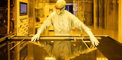
The Netherlands based roll-to-plate nano-imprinting technology developer Morphotonics announced that it has secured its Series B funding round, raising over $10 million from 3M New Growth Ventures, BOM and Innovation Industries. The company expects to add to this round and close it by the end of the year.

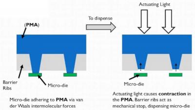
Morphotonics provides large-area nanoimprint systems, based on its unique roll-to-plate technology. The company's main markets are 3D displays and AR glasses. The company's technology can also be used as a flexible stamping system for microLED mass transfer.

Read the full story Posted: Sep 12,2024

MicroLED mass transfer technology innovations to be featured at MicroLED-Connect 2024

MicroLED-Connect is the world's first dedicated MicroLED conference and exhibition. The event, organized by TechBlick and the MicroLED Association, will take place at the High Tech Campus in Eindhoven, also known as "the smartest square kilometer in all of Europe", and will include an excellent conference program, masterclasses, tours - with a special emphasis on social/professional gatherings and networking opportunities. Register now and enjoy a discounted rate (until August 16).

MicroLED Connect Agenda 2024-09 image

A major challenge for microLED production lies at the mass transfer process, in which LEDs have to be transferred from the processed epiwafer to the final display substrate. A good mass transfer process has to be quick, efficient, and accurate - not an easy feat to achieve. MicroLED-Connect will present ample opportunities to learn more about transfer technologies, the challenges, the different processes and the latest innovations.

Read the full story Posted: Aug 05,2024

An interview with Justin Brown - X Display's Executive Vice President Operations & Equipment

Justin Brown is X Display's Executive Vice President for Operations & Equipment. Justin leads the company’s supply chain development, manufacturing partner relationships and also its Equipment division, which provides mass-transfer equipment for XDC’s partners and licensees. Justin was kind enough to answer a few questions we had for XDC.

Q: Hello Justin, thanks for your time. XDC has been a bit quiet in the last few years. Can you bring us up to date on your microLED technologies, processes and products?

Thank you for the opportunity to share the progress at XDC. We have been busier in the near past than ever before. As you know, we first announced our MicroIC technology, our mass transfer process, our manufacturing equipment and the uniqueness of our approach, the IP strength we possess and the experience of the team. This led to broad customer visibility and we narrowed down our efforts to a select set of partners that we are currently working with. We have deep engagements with customers that we anticipate will result in end product announcements in the future.

Read the full story Posted: Jul 03,2024

Micro-CPV: a promising new solar technology that may benefit from microLED production processes

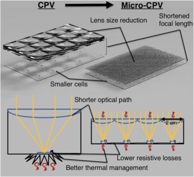
Researchers from the  Universidad Politécnica de Madrid and MIT, published a review article on Micro-Scale Concentrating Photovoltaics, or micro-CPV, a new technology that uses miniaturized solar panels and optics that concentrate the sun's energy into these micro panels. The benefits of micro-CPV compared to normal solar panels include potentially lower cost (much less solar absorption area), better thermal management, shorter optical path and lower resistive losses.

There are many challenges yet before micro-CPVs can be produced in large volume and at competitive prices. Interestingly, microLED production processes can be applied to the production of micro-CPVs, as these solutions can be seen like inverted technologies - tiny devices that either absorb or emit light.

Read the full story Posted: Nov 01,2023

TechBlick's upcoming microLED and QD event: Market Forecasts, QD-CMOS SWIR Imagers, Mass Transfer and more

TechBlick will soon host its virtual microLED and QD event, and here is a good preview of some of the technologies and advances that will be detailed during the event. MicroLED-Info readers enjoy a special discount to this interesting upcoming industry event.

We highlight important advancements in MicroLED and/or QD displays in this article using technology slides. These advancements of the art will be presented at TechBlick’s 2-day global conference on “Mini- & Micro-LED Displays: Markets, Manufacturing Innovations, Applications, Promising Start-ups” taking place online in TechBlick’s ‘in-person virtual’ platform on 30 Nov - 1 Dec 2022.

The agenda includes the likes of Samsung, Sharp, AUO, Coherent, ASMPT, Komori, CEA, Micledi, 3D Micromac, Allows Semiconductors, and many more. Full agenda can be seen here.

This conference is supported by the MicroLED Association.

Read the full story Posted: Oct 20,2022

MicroLED and QDs: Selected Technology Highlights by TechBlick

This is an article by TechBlick, organizers of the upcoming MicroLED Displays virtual event. MicroLED-Info readers get a 100 Euro discount.

In this article, using select technology slides, we highlight several interesting advancements in MicroLED and/or QD displays. More specifically, we cover 3600PPI “Silicon” Displays | Gravure printed microbumps | Electrohydrodynamically printed QD color converters | Laser LLO and Transfer for MicroLEDs | QD vs Phosphors | Energy saving credentials of microLED

“Silicon” Displays with an incredible 3600ppi full color using microLED and QD technology?

Sharp (HIRANO Yasuakie et al) has developed this technology.

As shown in the slide below, first blue-only uLEDs are formed on a sapphire substrate. Here, one LED array contains 352 x 198 micro LED dies of 24 um x 8 um in size. In parallel, an LSI chip containing the driving circuitry is formed on a silicon wafer. Here, the cathode (N-type electrode) and anode (P-type electrode) are fabricated for each micro LED die to apply driving voltage independently to each die. The Au bump electrodes are fabricated in accordance with the pitch of the LED dies. The two substrates are flip-chip bonded using Au-Au bonding. Here one can already see the parallel to the silicon and optoelectronic industry (vs. the traditional thin film display industry!). Next, the sapphire layer is removed via laser lift off. Finally, Cd-free quantum dots (green and red) are deposited atop the microLED dies to enable R G color conversion. This way one achieves RGB colors.
Read the full story Posted: Sep 21,2022

MicroLED transfer technology explained

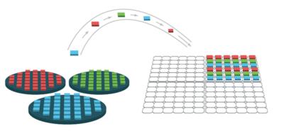
The microLED transfer process is crucial in MicroLED display production, this is likely to be the most challenging part of the entire process. In this article (an excerpt from The MicroLED Transfer Process Report), we'll give an overview of the transfer process, its challenges, and alternatives.

microLED transfer process image

At the beginning of this stage, there's the wafer with the MicroLED chips, and a display substrate with the backplane TFTs on top. As we said, this is a challenging process, and there are three main challenges in this step – accuracy, speed and reliability.

It is important to note that if the display is based on RGB microLED devices, it complicates this step further – which is why many MicroLED makers are expected to adopt blue LEDs with color conversion.

Read the full story Posted: Feb 05,2022 - 4 comments

Measuring and Correcting MicroLED Display Uniformity

This is a sponsored post by Radiant Vision Systems

Introduction

MicroLEDs (micro-LEDs, mLEDs, or μLEDs) continue to demonstrate performance advantages for displays, ushering in a new generation of backlit and direct-view illumination technology. MicroLED displays consist of an array of microscopic LEDs (light emitting diodes) that form the display’s individual subpixel elements. This inorganic emissive technology offers many benefits over rival display technologies, including higher brightness and contrast, wider color gamut, and higher pixel density. MicroLEDs enable improved visual performance in ambient-light conditions, from total darkness to full daylight and when viewed from multiple viewing angles. These qualities make microLEDs especially attractive for applications such as mobile phones and watches, augmented- and mixed-reality (AR/MR) headsets, automotive display panels, and digital signage. 

Challenges associated with manufacturing high-quality microLED panels continue to hinder production efficiency and must be addressed before manufacturers can achieve commercially viable microLED display products. Producing displays with the level of visual quality customers expect while keeping component and production costs low demands quality control solutions that reduce waste while increasing yield of acceptable displays.

Read the full story Posted: Feb 17,2021

XDC installs the world's first 300mm elastomer stamp based microLED transfer tool

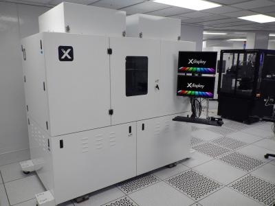
MicroLED display technology developer X Display Company (XDC) announced that it installed the world's first 300 mm elastomer stamp based mass MicroLED transfer equipment late in 2020. This tool was installed in the US and the company hopes to start shipping several similar tools for its customers later in 2021.

X-Display Corp 300 mm microLED transfer equipment photo

XDC spun out of X-celeprint in 2019 and retained the equipment organization from that transaction. XDC has over 15 years of experience with mass transfer micro printing technologies, and is offering a range of tools for microLED transfer, suitable for R&D work and industrial-scale production.

Read the full story Posted: Feb 04,2021 - 2 comments

VerLASE reports it has achieved substantial progress in its micro-LED display transfer technology

US-based parallel microLED assembly technology developer VerLASE Technologies reports today that it has achieved substantial progress in its mass transfer process for micro-LED displays.

VerLASE microLED transfer process scheme

VerLASE now plans to develop the process flow for an assortment of dies sizes from 200 X 200 um (mini-LEDs) down to 10 X 10 um and eventually also 5x5 um. VerLASE plans to demonstrate the transfer of both flip-chip, and vertical thin film LED architectures.


Read the full story Posted: Nov 01,2020