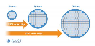
German-based GaN-on-Si developer ALLOS has applied its technology to large 300 mm epiwafers. ALLOS says that scaling up to 300 mm wafers enables higher production efficiencies and thus lower costs. ALLOS estimates that the higher area utilization alone accounts for a cost advantage of 40% compared to standard LED wafers. Standard 300 mm silicon line tools also offer higher production uniformity and yield.

ALLOS demonstrated the 300 mm scale-up using a reactor made by Veeco who announced selling the first 300 mm GaN reactor to a leading-edge semiconductor fab just some month ago and also showed 300 mm wafer data at CES. ALLOS reports a wavelength uniformity of consistently below 1 nm and "all other production requirements like bow of
We have discussed this achievement with ALLOS' co-founder, Alexander Loesing. While declining to give specific names, Alexander updates that the company is already working with leading display makers on adopting GaN-On-Si technology for MicroLED display production. Two names publically known to have a license of the GaN-on-Si technology are OSRAM and Epistar.
Alexander says that GaN-On-Si could help accelerate MicroLED development as it offers better uniformity compared to production on Sapphire wafers - the leading platform for conventional LED production today. Silicon also enables larger wafers which is a must to reduce production costs. Currently it is not possible to scale Sapphire wafers to 300 mm like it is for silicon.

