GaN-on-Silicon - Page 4

Aledia raised $36 million from Intel Capital and existing investors

Aledia logoFrance-based 3D GaN LED developer Aledia announced its Series-C Financing round, totaling $36 million. Its existing investors participated in this round, and Aledia also announced that Intel Capital has joined as a new investor.

Aledia also says that it is developing next-generation Micro-LED displays with several large industrial partners. Aledia is developing both mobile displays (for smartphones, tablets, etc) and micro displays for AR/VR applications.

Read the full story Posted: Feb 07,2018

Seren Photonics completes the first tranche of a £1 million investment round

Seren Photonics logoUK-based Seren Photonics has successfully completed the first tranche of a £1 million investment round with funding from existing and new investors. Seren says that these funds will be used to continue the manufacturing scale-up of its template technology along with the further development of green LED epitaxy structures.

Seren develops a suite of long wavelength LED epitaxy on its novel semipolar GaN aimed at delivering higher efficiency and more color stable green, yellow and red devices. Seren says that its Semipolar enabled LEDs overcome shortcomings of green LEDs manufactured on polar GaN, mainly low wall plug efficiency and poor poor wavelength stability over a range of current densities.

Read the full story Posted: Feb 07,2018

Researchers use a micro-LED covered with perovskite QDs to achieve high-speed visible light communication

Researchers from Fudan University, Shanghai develop a high-bandwidth white-light based system made from a blue gallium nitride (GaN) micro-LED with a yellow-emitting perovskite quantum dots. This system could be a way to enable high-speed real-time visible light communication (VLC).

The researchers used a 80 x 80 um blue-emitting micro-LED that has a modulation bandwidth of about 160 MHz and a peak emission wavelength of ~445 nm. The white-light system (following the perovskite QD conversion) achieves 85 Mhz - which means a maximum data rate of 300 Mbps.

Read the full story Posted: Jan 19,2018

Veeco and ALLOS demonstrate 200mm GaN-on-Si wafers for micro-LED production

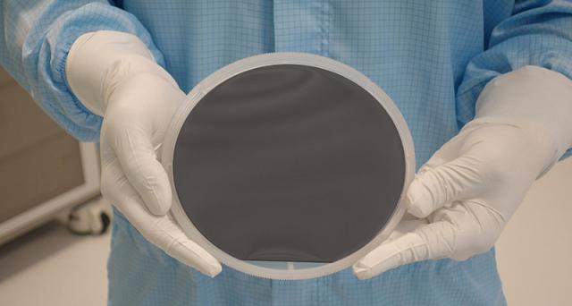
Veeco and ALLOS Semiconductors have completed their micro-LED strategic initiative and demonstrated 200mm GaN-on-Si wafers for blue and green micro-LED production. Veeco transferred ALLOS' proprietary epitaxy technology onto Veeco's Propel Single-Wafer MOCVD System to enable micro-LED production on existing silicon production lines.

ALLOS GaN-on-Si wafer photo

ALLOS says that it now has an MOCVD technology that is capable of high yielding GaN Epitaxy that meets all the requirements for processing micro-LED devices in 200 millimeter silicon production lines. Within one month the two companies managed to establish the ALLOS technology on Veeco's Propel systems and have achieved crack-free, meltback-free wafers with less than 30 micrometers bow, high crystal quality, superior thickness uniformity and wavelength uniformity of less than one nanometer.

Read the full story Posted: Nov 02,2017

glō orders an MOCVD tool for Aixtron to deposit GaN nanowire-based Micro-LEDs

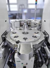
Swedish-American GaN nanowire based micro LEDs developer glō ordered an AIX G5+ MOCVD platform from Aixtron to support the company's strategic expansion. The tool will be delivered with a 8x150 mm configuration by the end of 2017.

Aixtron G5+ MOCVD handler photo

glō is commercializing micro-LED products based in its proprietary defect-free GaN nanowires technology. glō says that its technology enable the growth of mLEDs while maintaining the reliability of an inorganic material system.

Read the full story Posted: Sep 20,2017