Technical / research - Page 7

Researchers develop a new method to transfer and bond microLED arrays on flexible plastic substrates

Researchers from the University of Waterloo in Canada developed a new transfer and bonding method to deposit a flexible microLED array on plastic substrates.
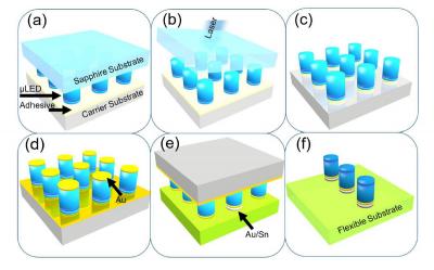
Flexible microLED paste-and-cut technique schema, University of Waterloo

The technique, referred to as a "paste-and-cut", starts with temporarily bonding the LEDs on a process/handle wafer onto a glass substrate (the paste step). The LEDs are then released (cut) to the flexible substrate. This approach allows the LED to be optimized and then combined with other materials.
Read the full story Posted: Jul 11,2020

Sapphire nano-membranes enable higher-efficiency microLEDs

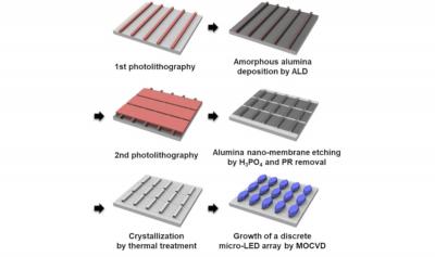
Researchers from Seoul National University (SNU) in collaboration with KAIST, SAIT and the Korea Photonics Institute developed a new method to deposit MicroLEDs on sapphire nano-membranes which enables chip singulation without an etching process. This method can enable higher efficiency MicroLED devices.

MicroLEDs grown on sapphire nano-membranes (SNU)

The researchers say that this method improves the internal quantum efficiency (IQE) of the microLEDs by 44% compared to standard GaN microLEDs produced on regular planar substrates. The microLEDs also featured a reduced dislocation density (by 59.6%). According to their tests, the microLEDs provided 3.3X the photoluminescence compared to regular microLEDs.

Read the full story Posted: May 11,2020

Researchers develop a new method to deposit high-brightness green InGaN microLED arrays

Researchers from the University of Sheffield a new fabrication process for green InGaN microLEDs that achieves high brightness compact microLED arrays.

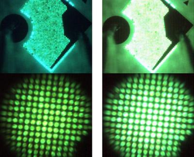
Emission microscopy of efficient InGaN green microLEDs (University of Sheffield)

Today most green InGaN microLEDs are produced by combining a standard photolithography technique with subsequent dry-etching processes on a standard III-nitride LED wafer. The researchers found a way to avoid the dry-etching processes which damage the surface the resulting LEDs. In the new process, the InGaN stack is direectly grown within pre-patterned micro-hole arrays through a thin (500nm) SiO2 layer serving as a GaN template over the epitaxial wafer.

Read the full story Posted: Jan 24,2020

The Perovskite Handbook - 2020 edition

MicroLED-Info and Perovskite-Info are happy to announce the 2020 edition of The Perovskite Handbook. This book is a comprehensive guide to perovskite materials, applications and industry, and it is now updated to January 2020 and lists recent developments and new companies, initiatives and research activities.

Perovskites are an exciting class of materials that feature a myriad of exciting properties. Perovskites are now entering the display market, with applications in quantum dots, LEDs, lasers and more.

The Perovskite Handbook

Reading this book, you'll learn all about:

  • Different perovskite materials, their properties and structure
  • How perovskites can be made, tuned and used
  • What kinds of applications perovskites are suitable for
  • Perovskites Quantum Dots
  • Perovskite solar cells, their merits and challenges
  • Perovskites-based LEDs
  • The state of the perovskite market, potential and future
     
Read the full story Posted: Jan 20,2020

iBeam Materials shows how to deposit both FETs and microLEDs directly on flexible metal foil substrates

iBeam Materials announced that it had successfully demonstrated the ability to produce high-performance GaN Field-Effect Transistors (FETs) directly on thin, flexible and rollable metal foil substrates.

This new technology complements iBeam's microLED deposition technology (demonstrated in the video above), and these FETs can be integrated with microLED chips in a side-by-side architecture. Both FETs and MicroLEDs are deposited on the flexible substrate without any transfer process.

Read the full story Posted: Jan 19,2020

Korean companies develop packaged RGB microLED technology for easier transfer process

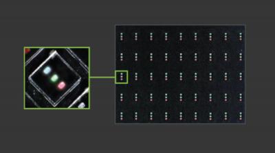
Seoul Viosys and Seoul Semiconductors have jointly developed a new MicroLED technology, called Micro Clean LED that basically packages three separate LEDs (red, green and blue) into a single "one-single MicroLED pixel".

Seoul Viosys Micro Clean Display photo

The idea is that these packaged colored pixels will be easier to transfer to the target substrate compared to the transfer of three different LEDs. The package itself does not contain any driver ICs.

Read the full story Posted: Jan 08,2020

KAIST researchers use 3D stacked MicroLEDs to enable high density displays

Researchers from the Korea Advanced Institute of Science and Technology (KAIST) developed a new process that enables the fabrication of highly dense MicroLED displays - up to 63,500 PPI (!).

The technique involves stacking RGB LEDs in three dimensions and a semiconductor patterning process. Stacking LEDs one on top of the other creates color interference issues, and to overcome this the researchers deposited an insulating film between the layers. This also improved the efficiency of the microLED devices.

Read the full story Posted: Jan 08,2020

Plessey develops the world's first InGaN on Silicon red LED

UK-based GaN-On-Si MicroLED microdisplay developer Plessey Semiconductor announced that it has successfully developed the world’s first GaN on Silicon-based Red LED.

Plessey native red InGaN LED, on silicon photos

Red LEDs are typically based on AlInGaP materia, or are color-converted from blue LEDs. These red LEDs limit the efficiency and the ability to create ultra-fine pitch sub pixels. Plessey says that InGaN red LEDs will also offer lower manufacturing costs, scalability to larger 200 mm or 300 mm wafers and better hot/cold factor over incumbent AlInGaP-based Red.

Read the full story Posted: Dec 06,2019

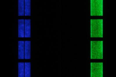
Plessey developed a process to deposit native green and blue microLEDs on the same wafer

UK-based GaN-On-Si MicroLED microdisplay developer Plessey Semiconductor announced that it managed to deposit native blue and green microLEDs on the same wafer. Plessey’s new patented process forms microLEDs that exhibit high current density operation and long operational lifetime.

Plessey native green and blue microLEDs wafer photo

Plessey said that to achieve this important milestone they had to overcome several challenges - including a magnesium memory effect, diffusion from the p-type cladding of the lower junction into the upper junction and the requirement for the precise tuning of the thermal budget during the growth of the second junction to prevent indium phase separation in the blue active region.

Read the full story Posted: Oct 06,2019