Finland-based Comptek Solutions develops passivation technology solutions for III-V compound semiconductor materials and devices, based on its novel surface treatment process. Comptek's research leader Marjukka Tuominen will give a talk at the upcoming MicroLED-Connect startup showcase event on February 2024, and Comptek's CEO and co-founder, Vicente Calvo Alonso, was kind enough to send us a short update on the company's technology and status, and his views on the microLED industry and market.
Q: Hello Vicente, thank you for your time. Can you tell us a bit about Comptek, your technology and current status?
Comptek Solutions is an expert in passivation technology solutions for III-V compound semiconductor materials and devices. With our novel surface treatment process, KontroxTM, we are able to control how the oxidation process happens on the surface of the compound materials, and for the first time ever, we can create high quality, crystalline native oxides which are thermodynamically stable and present very low levels of surface state defects.
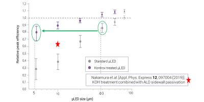
In microLEDs, Kontrox is applied to the chip mesa sidewalls, curbing non-radiative recombination mechanisms and effectively passivating the surface. This transformative approach leads to significant enhancements in the performance and manufacturing yields of µLEDs, particularly at small chip sizes. The outcome is a power-efficient microLED display with improved overall performance and pixel sizes.
But microLED is just one application of our technology, which is applicable also to a wide range of III-V materials and devices, such as lasers, detectors, power electronics, and RF devices.
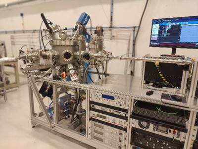
For example, we've successfully developed our passivation technology for treating edge emitting laser facets, and for this, we have designed and built our first proprietary passivation tool specifically tailored for the unique requirements of edge-emitting lasers.
The turnkey laser facet passivation tool developed by the Comptek team is the first in the market specifically optimized for edge-emitting laser applications.
Q2. What are the next steps for Comptek? What is your go-to-market strategy in the microLED industry?
In addition to lasers, we have been working a lot in microLEDs, for different materials based on GaN and GaAs. For one particular application of microled and for a particular set of materials, we have recently entered into a long-term development agreement with a renowned industry player. Currently, we are considering different applications where to establish additional collaboration. This could be, for example, automotive displays or large TVs.
We have also demonstrated that our technology can generate up to 2.5x improvement in mini LEDs, where our process efficiently treats not only the side walls but also the top surface.
Such substantial performance improvements can enable display manufacturers to reduce chip size, subsequently lowering costs and potentially accelerate market penetration.
Effect of Kontrox passivation on external quantum efficiency (EQE) across various GaN-based µLED chip sizes.
Q3: What do you feel are the main challenges for the microLED industry and market today?
Clearly, many technological challenges remain on the path to realizing mass production of microleds, translating into low production yields and exceedingly high costs. Therefore, any technology capable of mitigating these manufacturability and yield challenges and reducing costs would exert a tremendous impact.
Q4: What are your thoughts regarding the microLED market at this stage? How close are we to commercialized microLED displays?
Well, there are currently some microLED showcases in the market, but with exorbitant prices. Despite ongoing rumours about the mass production of smart watches for several years, consistent delays in their launch indicate unresolved issues. This underscores the complexity of the challenges at hand, with various approaches being explored to solve the same problems. It remains an open question as to who and what will be the winning horse in this race.
My personal bet is that around 2025, we might be able to see the first microLED products with certain volumes emerging in the market.
Q5: Many say MicroLED will disrupt the display value chain because it is not just an evolution of existing display technology. How do you see the changes and how will that impact Comptek's position in the industry?
It seems clear that, based on the theoretical properties of microLEDs, once we are able to produce them in significant volumes and at reasonable costs, microLED displays will surpass others in the market. This stands true even in light of recent advances and improvements that are being achieved in OLED technology.
As you’ve noted, microLEDs will disrupt the display market value chain, given that the primary component of the display is now a semiconductor. This shift represents a completely new landscape, and traditional display manufacturers do not necessarily have the in-house knowhow to navigate it.
Currently, OLED stands as the state of the art display technology, dominated by a Korean company. In the early days of OLED development, there were different players developing OLED displays, with different approaches or technology bets, such as white OLED vs RGB,etc. Those developments were carried out by display manufacturers with a strong affinity for LCD displays, and where some of their existing infrastructure could still be utilised. In the end, practically only one company succeeded in developing and mastering the technology.
For display manufacturers relying solely on LCDs, if they want to keep up and survive, they need to upgrade the technology. The step forward is OLED. Yet, this poses two significant challenges: the substantial investment required to build an OLED factory, amounting to several billion dollars, as well as the prolonged and intricate process of mastering the technology.
On the contrary, building a fab for microLEDs could be a more cost-effective option. Considering the technology is in its early stages for everyone, this presents an opportunity for companies to enter the next generation of display technology with much less investment. However, the type of suppliers and the entire value chain for microLEDs differs a lot from the existing display value chain. This clearly brings opportunities to many companies like Comptek, where individual and novel technologies addressing specific aspects and issues of the whole manufacturing flow could play crucial roles in a larger puzzle that will be manufactured in massive volumes in the end. In sum, the new value chain, resembling more of a semiconductor model, creates a significant synergy for Comptek's passivation technologies.
Thank you Vicente, looking forward to hearing Comptek's lecture in February!


