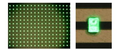
Toray Industries announced that it has developed a new conductive bonding material that works at lower temperatures (110 degrees Celsius) and pressures (5 megapascals) compared to existing materials, and is suitable for microLED processes.
Toray's new material is based on the company's RAYBRID photodefinable conductive material (produced from metals, glass, ceramics and other materials), combined with nanocarbon and adhesives. The company plans to start producing the new material by early 2025.
Bonding microLED chips to the display substrate is a challenge as these chips are very small, and the process needs to be quick and accurate. Toray said that photolithography can be used to form bumps from the new material, with diameters as small as 5 micrometers. The material can be re-formed using lasers, and so is suitable to be repaired using laser-based processes.


