ams OSRAM to expand its LED production plant in Malaysia, will be used to produce microLEDs on 8-inch wafers
ams Osram announced that it will expand its LED production plant in Kulim, Malaysia, with an investment of around $850 million.

The new fab will produce LED chips and microLED chips, on 8-inch wafers. ams Osram regards microLED as one of its key initiatives, but also sees the market a few years away.
ams Osram: microLED is one of our key initiatives, but the market is a few years away
In a recent conference call, Alexander Everke, the CEO at LED and sensor developer ams Osram, remarked that microLED is one of the company's key initiatives.
The microLED market, according to Everke, is "clearly a few years away", but the company plans to invest in the technology to make sure it stays ahead of the curve, as it wants to position itselff as the clear microLED leader.
Kyocera and OSRAM suggest hybrid PWM-current driving for microLED displays
Kyocera and OSRAM have jointly designed a new hybrid current and PWM driving technology for microLED displays. The two companies says that this new driving scheme can be used to avoid using lower pixel currents through microLED chips, which reduces the deviation of the luminance and the color shift at lower grayscale levels.

Kyocera has presented a 3.9" full-color microLED display on an LTPS backplane that showed excellent performances that proves the validity of the new driving technology.
ALLOS Semiconductor sells its HPE and RF business, to focus on the microLED market
German-based GaN-on-Si developer ALLOS announced that it has sold its high-power electronics and RF business to AZUR SPACE. ALLOS will now focus its business on the microLED display market.
ALLOS Semiconductors developed its GaN-on-Si epiwafer technology for both high power electronics and Micro LED applications, but the time has come to focus on one market. The company says its 200 and 300 mm epiwafer technology is crucial in meeting the uniformity, crystal quality and manufacturability requirements of the novel Micro LED display applications.
ALLOS and Veeco up-scale GaN-on-Si microLED production technology to 300 mm wafers
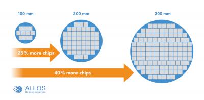
German-based GaN-on-Si developer ALLOS has applied its technology to large 300 mm epiwafers. ALLOS says that scaling up to 300 mm wafers enables higher production efficiencies and thus lower costs. ALLOS estimates that the higher area utilization alone accounts for a cost advantage of 40% compared to standard LED wafers. Standard 300 mm silicon line tools also offer higher production uniformity and yield.

ALLOS demonstrated the 300 mm scale-up using a reactor made by Veeco who announced selling the first 300 mm GaN reactor to a leading-edge semiconductor fab just some month ago and also showed 300 mm wafer data at CES. ALLOS reports a wavelength uniformity of consistently below 1 nm and "all other production requirements like bow of
Osram and the Fraunhofer IISB to co-develop MicroLED for automotive applications
The Germany Bavarian state ministry for regional development has funded a new three-year project to develop transparent micro-LED displays for automotive applications.

The SmartVIZ project consortium consists of Osram, Fraunhofer IISB and ASM Amicra. The partners aim to develop direct-view high-resolution transparent and demonstrate a prototype in October 2021.
Pagination
- Previous page
- Page 2


