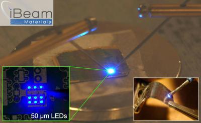
US-based iBeam Materials develops a technology that uses ion-beam to grow microLED devices on a variety of large-area substrates, including thin, flexible large-area metal foils. iBeam's founder and president, Vladimir Matias, will give a talk at the upcoming MicroLED-Connect startup showcase event on February 2024, and he was kind enough to send us a short update on the company's technology and status, and his views on the microLED industry and market.
Hello Vladimir, thank you for your time. Can you tell us a bit about iBeam, your technology and current status?
iBeam Materials is an early stage technology company developing a revolutionary approach to the epitaxial semiconductor growth process required for making LEDs and microLEDs such as in the next generation of displays. Instead of GaN crystal growth on expensive, rigid single crystal substrates that are limited in size, iBeam technology allows growth of the same high-quality semiconductor material on large-area, low-cost metal foil that permits roll-to-roll processing due to its flexibility.
This flexible substrate can follow all the way into a display product, for example, and the large areas and low costs mean monolithic integration is feasible for displays the size of cell phones or even larger, where integration of the driver ‘backplane’ into the same epitaxial material as used for the LEDs is possible. Already we have demonstrated GaN-based transistors in this material, as well as the LEDs themselves of course. We expect to use color-converting quantum dot films to achieve full-color display demos, or any of the same alternative technologies demonstrated by other approaches to achieve full color are also possible.
The critical interface layers required for single-crystal epitaxial growth on a polycrystalline or amorphous substrate are made by a patented process called ion-beam assisted deposition (IBAD), pioneered by iBeam’s founder Vladimir Matias. This process has been successfully used by the high-temperature superconductor industry for many years, where superconducting tapes are manufactured by the kilometer daily. iBeam is instead adapting this process to disrupt the much larger GaN industry.
Currently iBeam is scaling up its roll-to-roll IBAD deposition process from the successful 12-mm technology-demonstration size to a 150-mm size good for prototyping. The end goal is to scale to 500-mm or even wider to accommodate larger display sizes.
What are the next steps for iBeam? What is your go-to-market strategy in the microLED industry?
Next steps are to complete the scale-up of the IBAD metal tape template used for crystal growth, and then bring the MOCVD crystal growth process in-house, rather than having to rely on a partner for that step as we have done so far. This will allow us to make the full LED structure and to advance our process development with rapid turn-around times and cycles of learning. With that new capability and custom R2R equipment, iBeam will be able to generate scaled-up prototypes that will be useful for collaboration with potential customers. We don’t envision ourselves becoming a display manufacturer, but rather selling large-area epitaxial sheets or rolls that can be processed into flexible displays. We may also license our process to other manufacturers. We expect to work closely with display partners to enable their success using this process.
What do you feel are the main challenges for the microLED industry and market today?
The key challenges continue to be cost, yield, and uniformity that prevent high-volume commercial microLED products from being released with 100% of the pixels working. A practical manufacturing process still has not been realized despite years of promises and delays that attest to these problems. In addition, with the current approaches that rely upon mass-transfer of discrete devices, no one is seriously able to pursue the biggest opportunity there is, that of cell-phone sized high-resolution displays. We feel that large-area, low-cost monolithic integration is the solution to these problems, in the same way that discrete devices were replaced by large-scale integration in the silicon industry. As displays acquire higher resolution and ultimately go to 3D displays in the future the mass-transfer approaches become even less practical in our view.
What are your thoughts regarding the microLED market at this stage? How close are we to commercialized microLED displays?
Rumors continue to abound as to when a high-volume consumer product will be released by a major manufacturer such as Apple, beginning most likely with a wearable product that has the benefit of small size and the need for low power consumption and high brightness. This would be an ideal first product for microLEDs, but it looks like it is still about 2 years out, as it has been for several years now! The microLED TVs that are already available remain a low-volume niche product due to their high prices, since a successful low-cost manufacturing approach still has not been identified.
Many say MicroLEDs will disrupt the display value chain because it is not just an evolution of existing display technology. How do you see the changes and how will that impact iBeam's position in the industry?
iBeam’s revolutionary approach in particular is highly disruptive to the supply chain for current microLED approaches. Our approach is actually more similar to current OLED architectures but could even be simpler than those. A completely monolithically integrated display would consist of LEDs and transistor devices all integrated within a single sheet, simplifying the displays of the future as well as making them flexible and paper thin. The potential benefits of this unique approach that differs from all the others means iBeam could become the market leader in the supply chain. We are planning for this success.
Thank you Vladimir, looking forward to hearing your lecture in February!


